Semiconductor Fab Complex in Austin
High-Tech Facilities Overseas
1996.05.01 ~ 2012.12.31
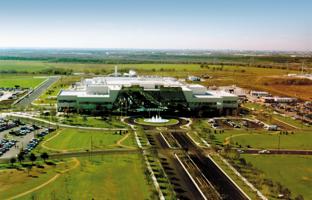
GFA: 1,155,000㎡
Decription: Located in U.S.A
[Hightech/Semiconductor production R&D]
The wafer fabrication plant is a three-story building with a total approximate area of 580,000 square feet. The plant mass-produces 64 mega-DRAM memory chip products. The facilities include 100,000 square feet of 0.1 µ, Class 1 cleanroom 45,000 square feet of sub-cleanroom which ranges Class 1 to Class 1000. In addition to the main fabrication building, a central utility plant, secondary substation, gas plant, deionized water system, bulk chemical distribution system, specialty gas system, wastewater treatment system were included. Site work encompassed grading, drainage, roadwork, retention ponds, lscaping.
The central utility building is approximately 75,500 square feet is comprised of a ground floor, a basement. The building contains most of the utility equipment central systems for the facility. The gas plant is approximately 4,800 square feet contains specially coated piping generation equipment. The secondary power substation is approximately 3,400 square feet houses the major electrical control system for the primary substation all other facilities. Miscellaneous structures include an underground culvert connecting the central utility building with the cooling tower gas plant, utility racks connecting the wafer fabrication plant with the central utility building, cooling tower, tower trenches, duct banks, scrubber pads, pits, foundations.
Samsung broke ground on March 28, 1996 with a directive to have all facilities constructed within a 16-month period. Utilizing fast track construction techniques first tool move-in was accomplished in June 1997, all employees were formally moved into the facilities on August 7, 1997, production began in October 1997.